
Kyma supplies Custom III-N Epiwafers both for materials studies and for a number of device applications, including light emitting diodes (LEDs), microwave / RF transistors, acoustic wave filters, photodiodes, and power switching.
Learn More
Kyma's external metal-halide sources enable a robust, cost-effective extension of existing crystal growth capabilities to enable new materials compositions.
Learn More
Kyma has over a decade of experience in fabricating crystalline wide bandgap semiconductor (WBGS) materials including GaN, AlN, Ga2O3, SiC, and sapphire. All of Kyma's wafer fabrication & substrate reclaim services are performed in-house in Kyma's fully equipped wafer fabrication facilities
Learn More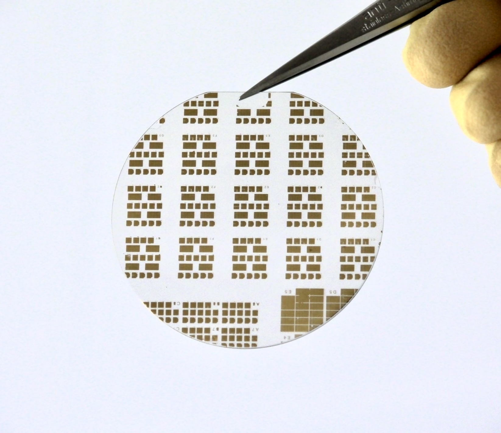
Kyma's ß-Ga2O3 epiwafers are grown on (010) ß-Ga2O3 substrates and have high electrical quality and also high structural quality that matches that of the substrate.
Learn More
Kyma offers (010) orientation single crystal gallium oxide (ß-Ga2O3) substrates (and epiwafers) to support the development of epitaxial growth and device development in this exciting new materials system.
Learn More
Kyma’s 200-mm HVPE GaN on QST® Templates consist of 10 microns of HVPE GaN grown on 200-mm diameter QST® substrates provided by Qromis, Inc.
Learn More
Kyma’s GaN on sapphire templates are available in diameters from 2" up to 8" or 200-mm and consist of a thin layer of crystalline GaN grown by HVPE on a sapphire substrate. Epi-ready templates now available...inquire today!
Learn More
Kyma’s GaN templates are available in diameters from 2" up to 8" or 200-mm and consist of a thin layer of crystalline GaN grown epitaxially by HVPE on a silicon substrate.
Learn More
Kyma's new c-plane GaN substrates have improved defect density, very low pitting, and is now available in 4”. This new generation of bulk GaN from Kyma is an excellent starting point for specialty lighting, laser diodes, and the burgeoning market of vertical GaN power electronics.
Learn More
Kyma's K200™ HVPE Growth Tool is the industry's first fully automated large diameter hydride vapor phase epitaxy (HVPE) growth tool.
The K200™ HVPE Growth Tool design benefits from hundreds of engineering advances achieved over 15 years of experience at Kyma in the application of HVPE to the growth of GaN, AlN, AlGaN and Ga2O3.

The KO-Switch™ is the highest power semiconductor switch of its size with a sub-nanosecond response time. Applications include electric circuit protection, pulsed power, ultra wideband (UWB) radar, and arbitrary waveform generation (AWG).
Learn More
Kyma customers benefit from Kyma's in-house suite of routine characterization tools and its quick access to local advanced characterization facilities.
Kyma also has rapid access to a number of advanced characterization tool at partner facilities in The Triangle for which Kyma staff is trained and certified to use.

Kyma's polycrystalline GaN (polyGaN) materials are useful for applications that require higher purity and/or lower surface area than legacy sources.
Learn More
Kyma's staff has multiple decades of accumulated experience in the design and manufacture of several types of vapor phase crystal growth tools for compound semiconductor materials growth.
Learn More
PureGaNtm is a breakthrough in GaN quality that unlocks the true versatility and value of vertical GaN power devices. Kyma's proprietary HVPE technology allows thick GaN films with extremely high chemical purity to be grown.
Learn More
Kyma’s PVD with Nanocolumns (PVDNC™) AlN templates, available in diameters from 2" to 12", consist of a thin layer of nanocolumnar crystalline AlN which was grown epitaxially by PVDNC™ on a sapphire or silicon substrate.
Learn More
Kyma’s UV Grade AlN on Sapphire Templates, available in diameters from 2" to 6", consist of a thin layer of high purity crystalline AlN which is designed to meet the demanding requirements of UVC LED applications.
Learn More
Kyma Technologies specializes in advanced wafer polishing services for crystalline wide bandgap semiconductor (WBGS) materials, including GaN, AlN, Ga2O3, SiC, and sapphire. With over a decade of experience and state-of-the-art equipment, Kyma has developed unique capabilities in controlling the crystallographic orientation and intentional mis-orientation of wafers during the polishing process.
Learn More