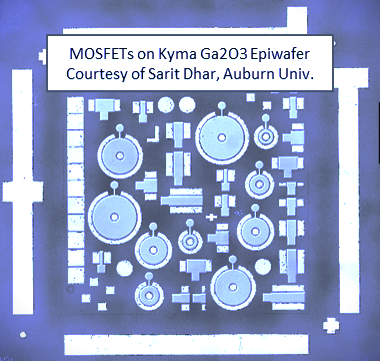
Crystalline β-Ga2O3 is an ultrawide bandgap semiconductor (4.8-4.9 eV) which exhibits breakdown fields as high as 8 MW/cm and a Baliga figure of merit 8x more than SiC and 4x more than GaN.
Kyma provides epitaxial Ga2O3 layers grown by Kyma’s proprietary halide vapor phase epitaxy (HVPE) technology or [coming soon] via metalorganic chemical vapor deposition (MOCVD), specializing in growth on (001) and (010) bulk substrates. Our epilayers have high structural quality that replicates the underlying substrates, and Kyma can provide thick lightly doped layers on (001) substrates (over 10µm thickness) with free carrier concentrations <1016 cm-3. Epigrowth can also be provided on substrates provided by Kyma in the (010) orientation or on customer provided substrates of other orientations.
We welcome requests on what is possible for custom thicknesses, doping schemes, or growth on alternative substrates up to 100mm in size.

Kyma offers (010) orientation single crystal gallium oxide (β-Ga2O3) substrates to support the development of epitaxial growth and device development in this exiting new materials system.
Learn More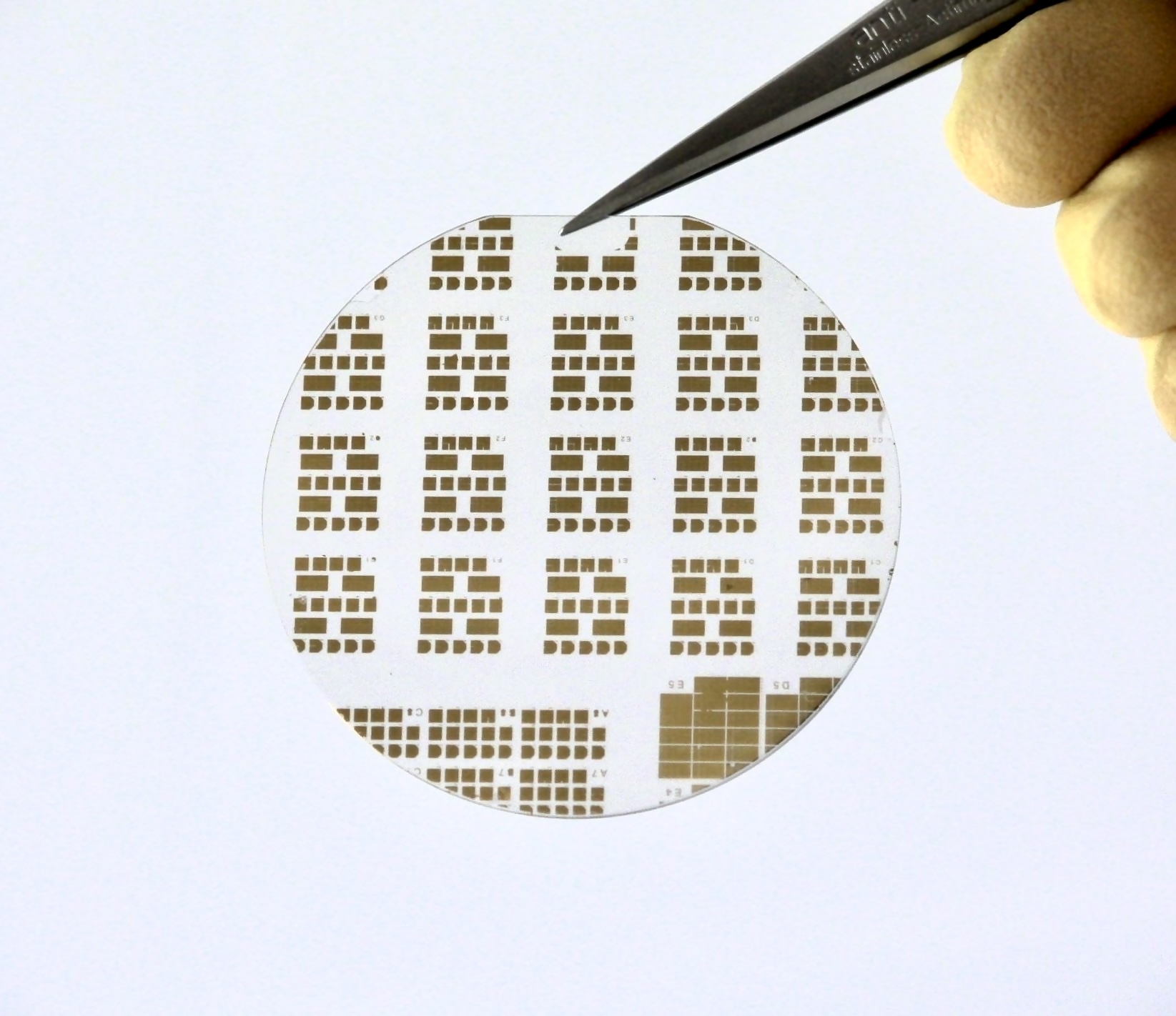
Kyma grows Ga2O3 epiwafers on bulk (001) and (010) β-Ga2O3 substrates with high structural and electrical quality for power electronics device applications.
Learn More