Gallium Oxide Epiwafers

Reach out to UsDownload Data Sheet

Gallium Oxide Epiwafers

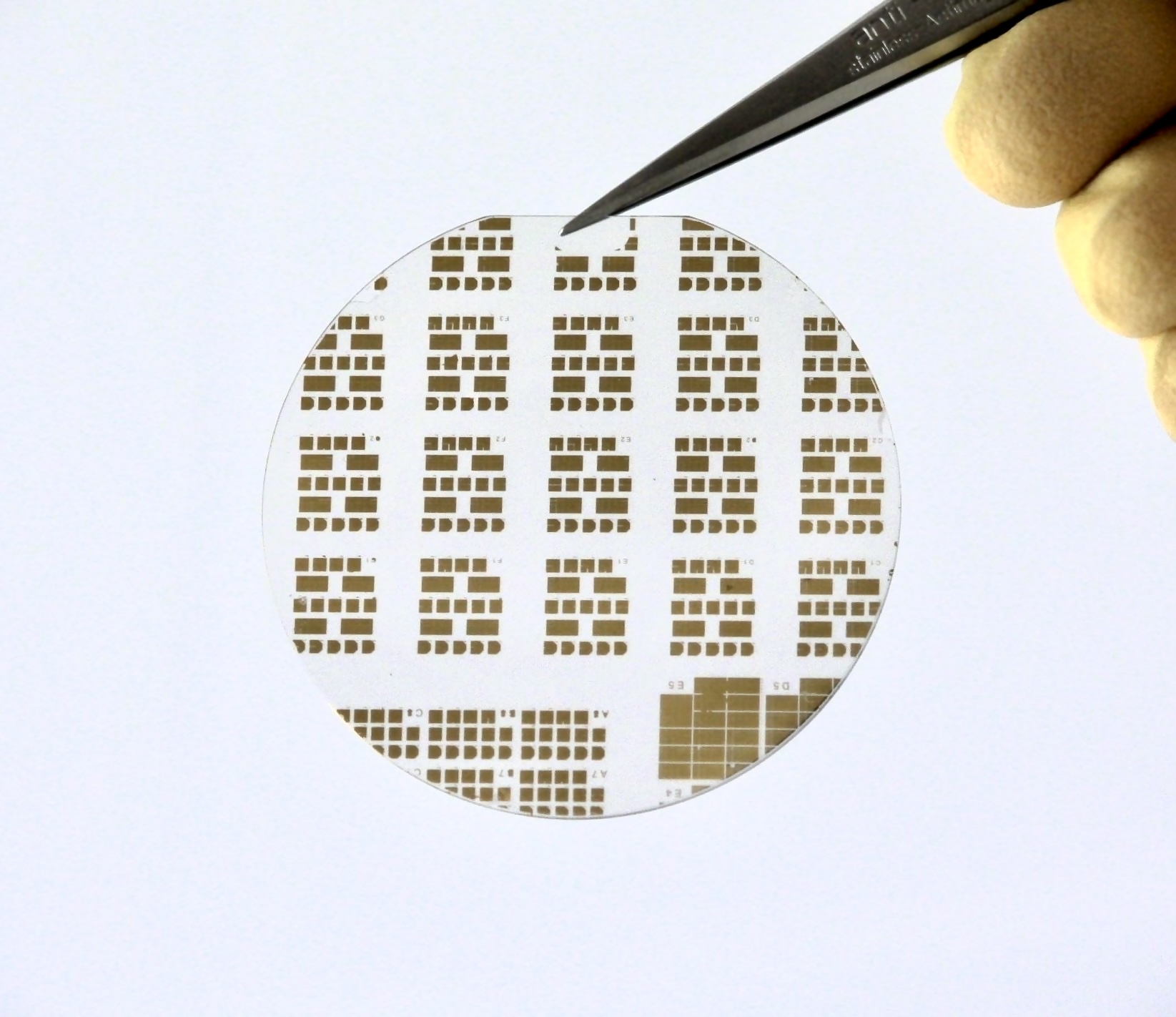
Kyma grows Ga2O3 epiwafers on bulk (001) and (010) β-Ga2O3 substrates with high structural and electrical quality for power electronics device applications.

Thick and lightly doped layers on bulk (001) substrates are now available for vertical device applications. The standard epiwafer configuration with a free carrier concentration of 1x1016 cm-3 and thickness of 10 microns is available on conductive 2" and 100mm (001) substrates, and additionally thicker and alternative doping concentrations are available upon request.

Customers can supply their own β-Ga2O3 substrates, or purchase directly from Kyma. Please reach out to start a discussion about what is possible.

Product Details

Features

  • High-quality β-Ga2O3 epilayers grown on β-Ga2O3 substrates
  • Exceptional structural quality matching the substrate
  • High room-temperature carrier mobilities exceeding 100 cm²/V·s
  • Low-temperature carrier mobilities up to 500 cm²/V·s
  • Customizable substrate options (customer-supplied or Kyma-provided)

Benefits

  • Enables high-performance power devices with improved efficiency
  • Supports high-voltage and high-power operation
  • Facilitates low-loss and high-frequency switching
  • Enhances device reliability and lifetime
  • Leverages Kyma's expertise in alternative substrate technologies

Applications

  • Power MOSFETs and switching devices
  • High-voltage converters and inverters
  • Solid-state circuit breakers and power distribution
  • Renewable energy systems (solar, wind)
  • Electric vehicle and traction drive systems

Knowledge Center