Kyma’s GaN templates are available in diameters from 2" up to 8" or 200-mm and consist of a thin layer of crystalline GaN grown epitaxially by HVPE on a silicon substrate.
For most of Kyma's GaN templates Kyma employs a patent-protected thin intermediate layer of crystalline PVDNC™ AlN between the GaN and the non-GaN substrate which serves as an excellent nucleation layer for GaN overgrowth.
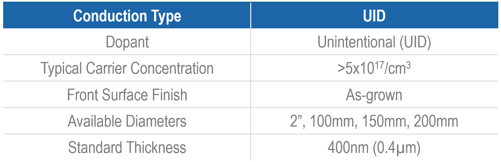
Customer benefits include 1) elimination of long (2-5um) MOCVD or MBE undoped buffer layer growth, and 2) the benefits of a "cleaner" buffer layer as HVPE GaN has higher chemical purity (no carbon!) and greater transparency than MOCVD GaN. Additionally, HVPE GaN can be grown faster and at lower cost than MOCVD GaN, due to a number of factors: HVPE growth can be carried out at 10x the growth rate of MOCVD, it uses less and lower cost starting materials (less NH3 usage, lower cost elemental Ga instead of metalorganic Ga), and the cost of an HVPE tool is typically less than that of an MOCVD tool.Below are Kyma's specifications for GaN on sapphire templates: